PCB & PCBA
Manufacturing Services

  1. Home
  2. /
  3. Products
  4. /
  5. PCB
  6. /
  7. PCB Products
  8. /
  9. HDI PCB
  10. /
  11. 14 layers second order...

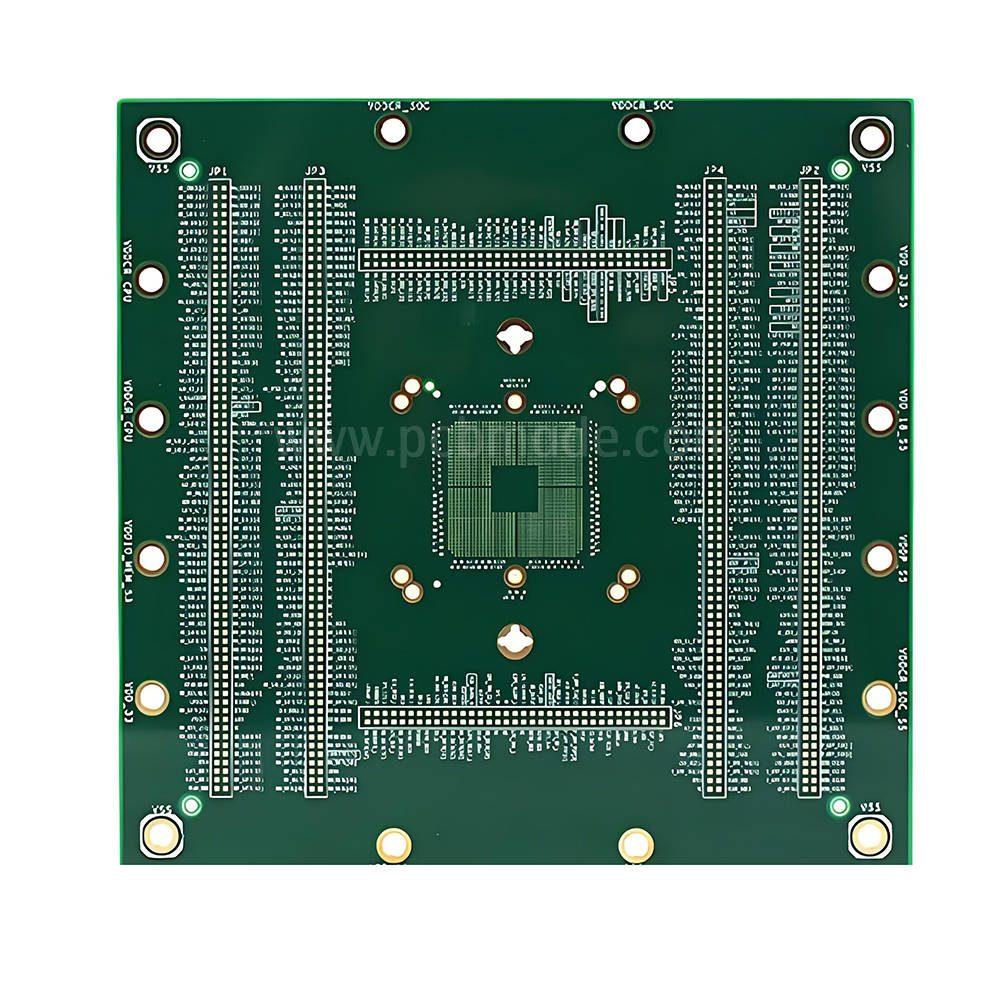
14 layers second order HDI plate

Product Parameters for 14-Layer Second-Order HDI Plate

Parameter Specification
Layer Count 14 Layers (2nd-order HDI structure with ​2 signal layers + 12 power/ground layers)
Material High-Tg FR4 (e.g., ​TG180) or ​Isola Tachyon for advanced signal integrity
Board Thickness 1.0mm–1.6mm (standard); ​0.8mm–2.0mm (customizable for compact designs)
Minimum Trace/Space 4mil/4mil (0.10mm/0.10mm) for high-density routing
Minimum Hole Size 6mil (0.15mm) laser-drilled vias (second-order HDI)
Aspect Ratio 8:1 (max) for blind/buried vias
Surface Finish ENIG (Immersion Gold) for solderability and corrosion resistance
Impedance Control 50Ω/100Ω differential pairs (±10% tolerance) for PCIe/USB4/DDR5 signals
Thermal Performance ΔT ≤ 3°C (10W/cm² heat load) with ​thermal vias and copper planes
Mechanical Strength Tensile Strength: ​100–150 MPa (FR4-based); ​180–250 MPa (high-Tg material)
Electrical Conductivity ~40 MS/m (copper traces with 1–2 oz copper plating)
Manufacturing Process Second-order HDI workflow: Laser drilling → Electroplating → AOI/X-ray inspection
Standards Compliance IPC-6012B (Class 10/12), ​RoHS 3.0, ​REACH, ​IPC-2221B
Applications Smartphones, ​high-end laptops, ​AI servers, ​5G base stations

14-Layer Second-Order HDI Plate | Ultra-Dense Interconnect Solutions for Advanced Electronics
Engineered for ​cutting-edge devices requiring extreme signal density and miniaturization, our ​14-layer second-order HDI plates deliver unparalleled performance in high-speed data transmission, power distribution, and thermal management. Built with ​high-Tg FR4 or ​Isola Tachyon substrates, these boards support ​blind/buried vias and ​micro-vias for compact designs while maintaining ​excellent signal integrity and reliability.


Key Features:

  • High-Density Routing: ​4mil/4mil trace/space enables ​100+ I/O per square inch for ​PCIe 5.0/USB4 Gen 2 applications.
  • Advanced Signal Integrity: ​50Ω/100Ω differential pairs with ​**<10dB insertion loss** at 24GHz for ​AI/ML accelerators and ​5G mmWave modules.
  • Thermal Efficiency: ​ΔT ≤ 3°C under high-power loads thanks to ​copper planes and ​optimized thermal vias for ​server GPUs and ​edge computing devices.
  • Mechanical Robustness: ​100–250 MPa tensile strength ensures durability in ​rugged laptops and ​industrial automation systems.
  • Precision Manufacturing: ​Second-order HDI process combines ​laser drilling (6mil vias) with ​electroplating for ​zero-crosstalk interconnects, validated by ​IPC-6012B Class 12 standards.

Ideal Applications:

  • Consumer Electronics: ​Ultra-thin flagship smartphones with ​foldable displays and ​under-display cameras.
  • Data Center Hardware: ​AI server motherboards with ​PCIe 5.0 x16 slots and ​DDR5 memory controllers.
  • Telecommunications: ​5G CPE devices and ​microwave backhaul units requiring ​high-frequency signal integrity (up to 60GHz).
  • Industrial IoT: ​Smart factories control systems with ​high-reliability connectors and ​EMC-compliant designs.

Why Partner With Us?

  • Customization: Tailored ​layer stack configurations (e.g., ​7 signal + 7 power layers) and ​impedance profiles for niche applications.
  • Cost Efficiency: ​Lean manufacturing reduces prototyping costs by ​30% with ​100% AOI/X-ray inspection for defect-free production.
  • Innovation: ​Graphene-enhanced substrates for ​20% improved thermal conductivity and ​nanoscale laser drilling for ​**±0.5mil via alignment tolerance**.

Elevate your next-gen electronics with 14-layer second-order HDI plates that balance density, speed, and reliability. Trust our expertise to power the future of high-performance computing and connectivity!

Related products

Contact Us