Key Features & Technical Specifications
- Ultra-Thin & Flexible Design:
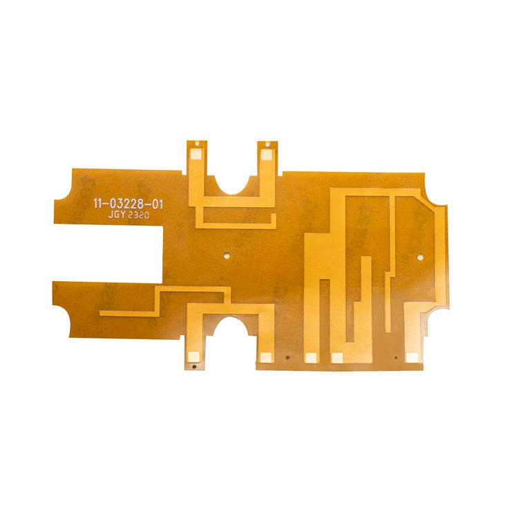
- 0.1mm thickness reduces device bulk by up to 40% compared to rigid PCB antennas, ideal for slim smartphones, wearables, or automotive dashboard installations
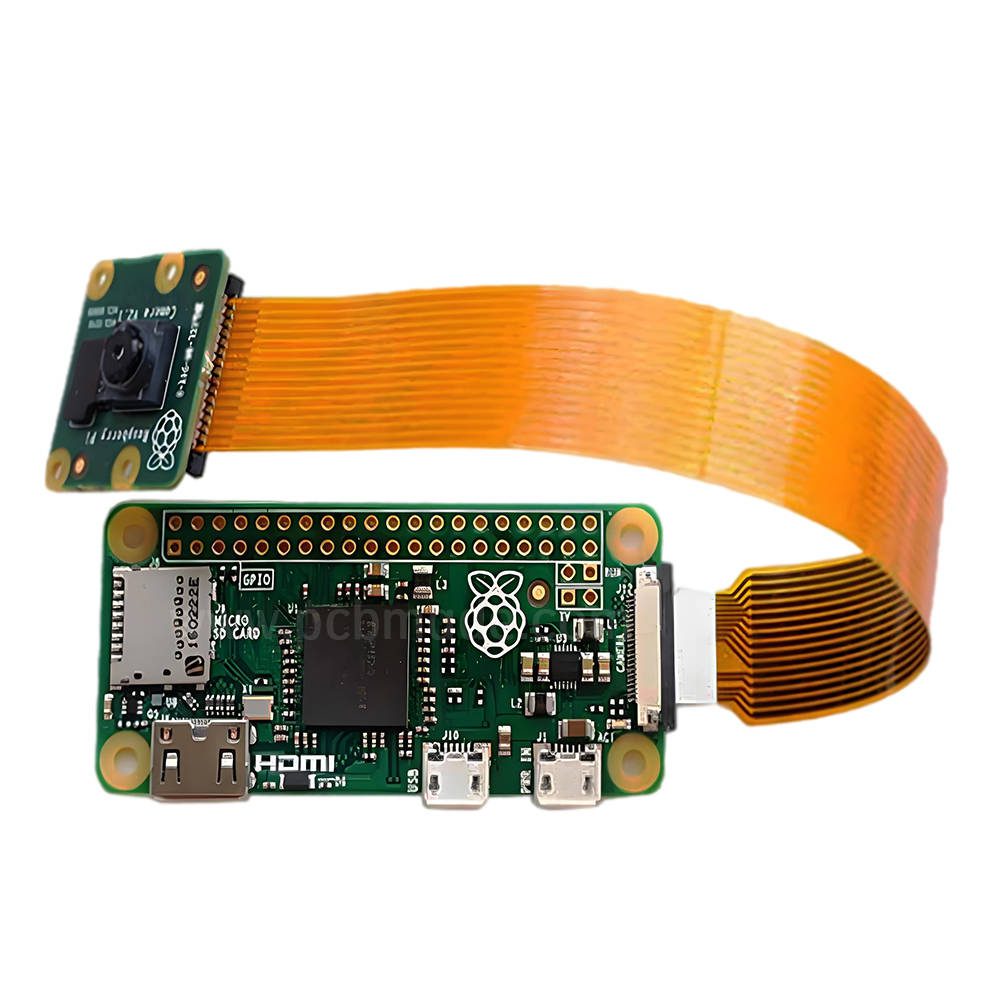
- Supports 90°–180° bending with a minimum bend radius of 0.5mm, enabling integration into curved casings or foldable devices
- High-Density Interconnects:
- Single-layer routing with 0.03mm/1mil trace width allows precise design of microstrip antennas, monopoles, or patch antennas for 2G–5G, Wi-Fi, and Bluetooth frequencies
- blind/buried vias enable compact layouts for integrated matching networks or embedded components
- Single-layer routing with 0.03mm/1mil trace width allows precise design of microstrip antennas, monopoles, or patch antennas for 2G–5G, Wi-Fi, and Bluetooth frequencies
- Signal Integrity & Performance:
- Controlled impedance (50Ω) ensures minimal signal loss for high-frequency transmission (e.g., mmWave 5G) and stable impedance matching
- Radiation efficiency up to 90% minimizes thermal losses in FR4 substrates, optimizing power transfer for battery-operated devices
- Controlled impedance (50Ω) ensures minimal signal loss for high-frequency transmission (e.g., mmWave 5G) and stable impedance matching
- Manufacturing & Design Tools:
- Designed using MATLAB Antenna Toolbox for parameterized geometry, array optimization, and 3D radiation pattern visualization
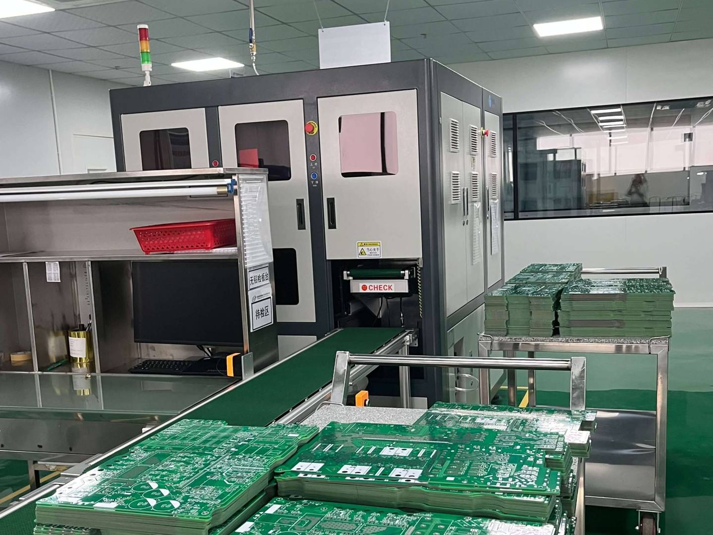
- Automated optical inspection (AOI) and laser drilling ensure precision in via alignment and defect-free production
- Designed using MATLAB Antenna Toolbox for parameterized geometry, array optimization, and 3D radiation pattern visualization
Applications
- Consumer Electronics:
- 5G-enabled smartphones, foldable devices, and smartwatches with embedded antennas
- Wearable fitness trackers and Bluetooth headsets with compact, durable antenna solutions
- 5G-enabled smartphones, foldable devices, and smartwatches with embedded antennas
- IoT & Smart Home:
- Wireless sensor nodes, smart lighting systems, and home automation hubs requiring long-range communication
- Wireless sensor nodes, smart lighting systems, and home automation hubs requiring long-range communication
- Automotive Systems:
- Vehicle-to-everything (V2X) communication antennas for connected cars and autonomous driving
- Dashboard-mounted antennas for GPS and AM/FM reception in electric vehicles
- Vehicle-to-everything (V2X) communication antennas for connected cars and autonomous driving
Advantages Over Rigid PCB Antennas
- Space Optimization:
- Replaces bulky wire harnesses or rigid PCB antennas, saving 30–50% in module volume and weight
- Enables 3D conformal packaging for curved surfaces or uneven device casings
- Replaces bulky wire harnesses or rigid PCB antennas, saving 30–50% in module volume and weight
- Design Flexibility:
- Simplifies integration with existing PCBs or enclosures using surface-mount technology (SMT)
- Supports dynamic interfaces for adaptive antenna configurations (e.g., beam steering in 5G arrays)
- Simplifies integration with existing PCBs or enclosures using surface-mount technology (SMT)
- Cost Efficiency:
- Reduces material waste by 40% compared to multi-layer rigid PCBs
- Lowers assembly costs through automated welding and reduced manual labor
- Reduces material waste by 40% compared to multi-layer rigid PCBs


