Key Features & Technical Specifications
- High-Density Interconnects:
- Multi-layer stack-up (up to 12 layers) with 0.03mm trace width allows for complex circuitry in compact devices (e.g., foldable smartphones, wearable sensors)
- Microvias (0.05mm) and blind/buried vias enable 3D routing without compromising signal integrity, ideal for high-speed data transmission (5G, mmWave)
- Multi-layer stack-up (up to 12 layers) with 0.03mm trace width allows for complex circuitry in compact devices (e.g., foldable smartphones, wearable sensors)
- Signal Integrity & Performance:
- Controlled impedance (50Ω–100Ω) ensures minimal signal loss in RF and high-speed applications
- Dedicated power/ground planes reduce EMI and improve power distribution efficiency, critical for electric vehicles and industrial equipment
- Controlled impedance (50Ω–100Ω) ensures minimal signal loss in RF and high-speed applications
- Thermal Management:
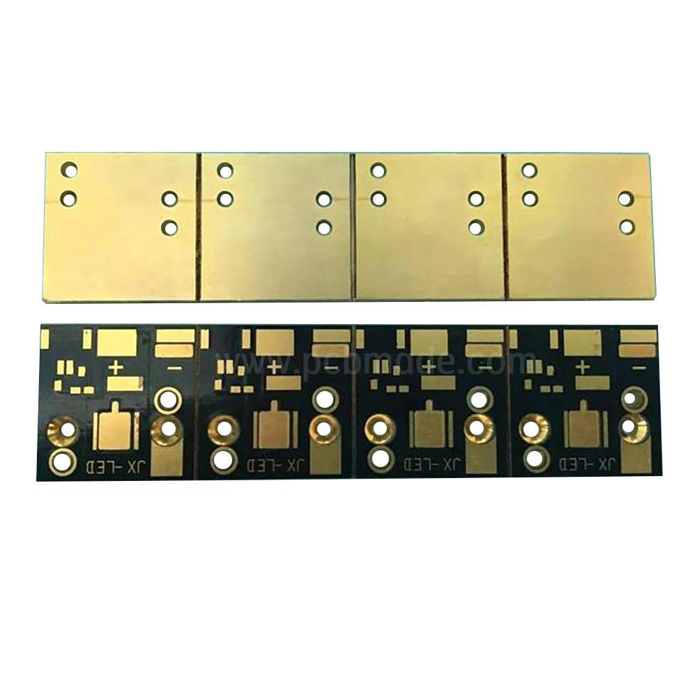
- Aluminum substrate (thermal conductivity up to 2.0 W/m·K) and phase change materials (PCMs) dissipate heat from high-power components, extending lifespan
- Aluminum substrate (thermal conductivity up to 2.0 W/m·K) and phase change materials (PCMs) dissipate heat from high-power components, extending lifespan
- Design Flexibility & Durability:
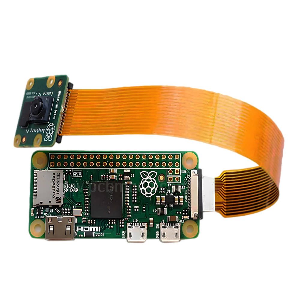
- Supports 90°–180° bending (minimum radius 0.5mm) for curved device casings or wearable tech
- IP67/IP68 certification and 10,000+ bend cycles ensure reliability in harsh environments
- Supports 90°–180° bending (minimum radius 0.5mm) for curved device casings or wearable tech


