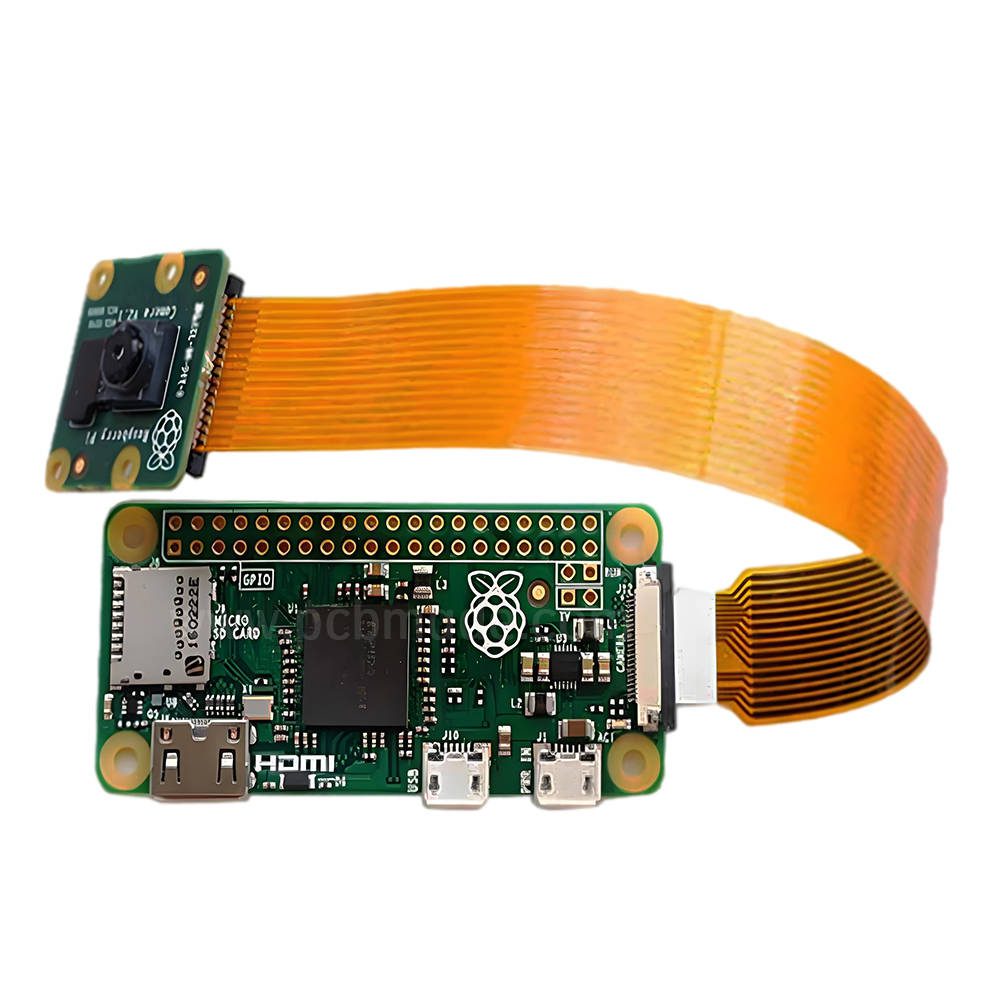

一、 What is PCB?
Printed circuit board (PCB) is a finished board made of insulating substrate and conductor materials, designed and manufactured with printed circuits, printed components or a combination of both according to a pre designed circuit schematic. Its main function is to use the insulating material on the board to isolate the copper foil conductive layer on the surface, realize the interconnection and relay transmission between electronic components, and enable the current to amplify, attenuate, modulate, decode, encode and other functions along the preset circuit in various electronic components, realizing the interconnection and relay transmission between electronic components.
二、 Classification of PCB
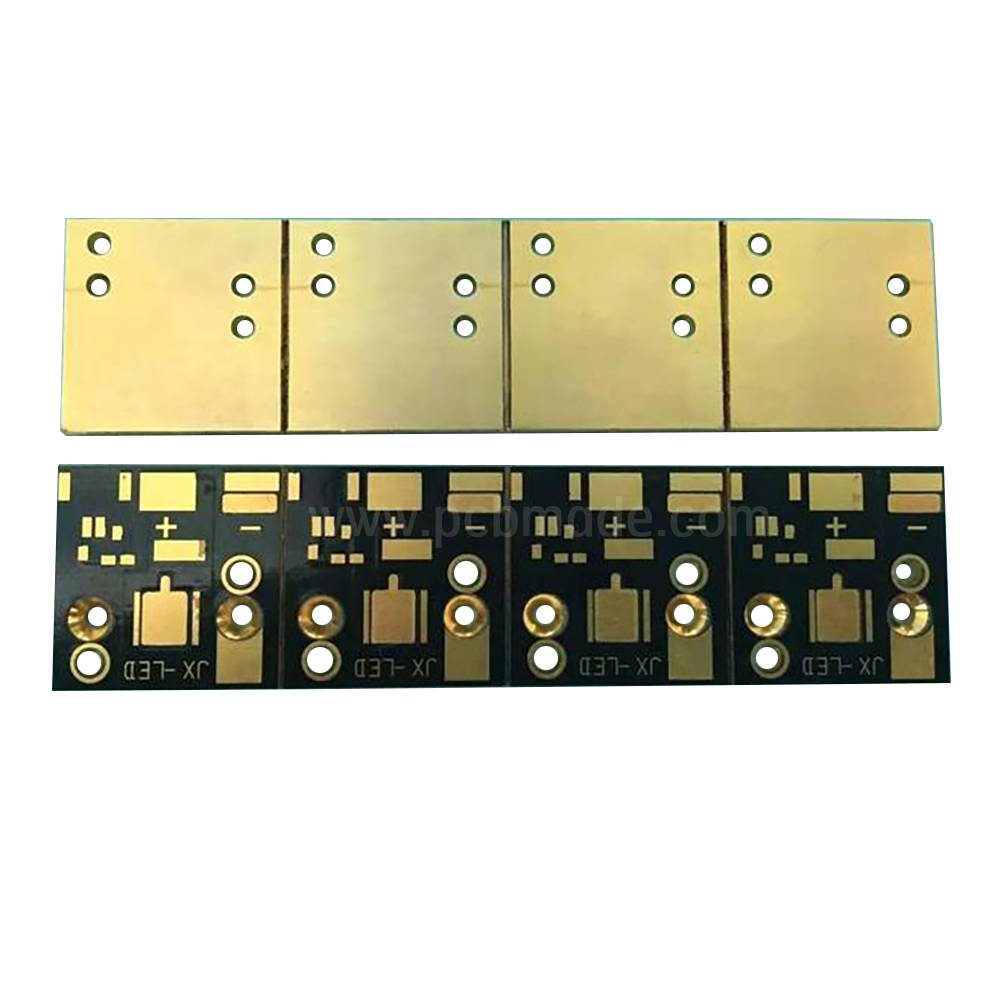
According to the bending toughness of the substrate used, it can be divided into rigid plates, flexible plates, and rigid flex plates;
According to the material, it can be divided into organic boards (phenolic resin, glass fiber/epoxy resin, polyimide, BT, etc.) and inorganic boards (aluminum substrate, copper substrate, ceramic substrate mainly depend on heat dissipation).
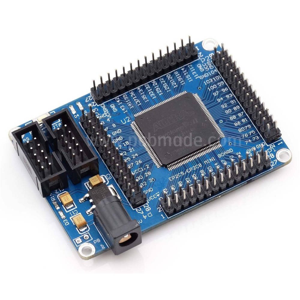
三、 Characteristics of Integrated Circuits
Integrated circuits have the advantages of small size, light weight, fewer lead wires and solder joints, long lifespan, high reliability, and good performance. At the same time, they are low-cost and easy to produce on a large scale. It is widely used not only in industrial and civilian electronic devices such as recorders, televisions, computers, but also in military, communication, remote control, and other fields. Using integrated circuits to assemble electronic devices can increase the assembly density by tens to thousands of times compared to transistors, and greatly improve the stable working time of the equipment.

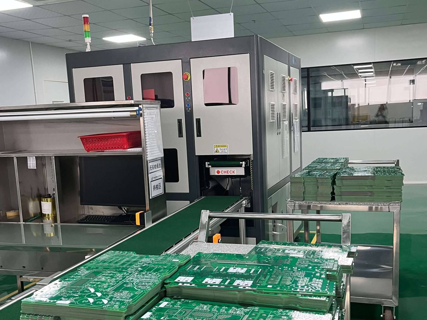
四、 The main components of PCB currently
The tool for conducting between the original components will be designed with a large copper surface as the grounding and power layer. The route and the map were created simultaneously.
(2) Dielectric layer: used to maintain insulation between circuits and layers, commonly known as substrate.
(3) Holes: Conductive holes can allow two or more layers of circuits to conduct with each other. Larger conductive holes are used as component inserts. In addition, there are non-conductive holes, which are usually used for surface mount positioning and fixing screws during assembly.
(4) Anti soldering ink: Not all copper surfaces need to be coated with tin on the parts, so non tin coated areas will be printed with a layer of material (usually epoxy resin) to isolate the copper surface from tin coating, avoiding short circuits between non tin coated circuits. The common inks are mainly green oil and blue oil.
(5) Screen printing: This is a non essential component and its main function is on the circuit board Label the names and location boxes of each component for easy maintenance and identification after assembly.
(6) Surface treatment: Due to the easy oxidation of copper surfaces in general environments, they cannot be tinned (poor solderability), so protection will be provided on the copper surfaces that need to be tinned. The methods of protection include tin spraying, gold plating, silver plating, and tin organic solder paste, each with its own advantages and disadvantages, collectively referred to as surface treatment.

五、 Characteristics of PCB board
(1) Can be high-density. For decades, high-density printed circuit boards have been developing with the improvement of integrated circuit integration and installation technology.
(2) High reliability. Through a series of inspections, tests, and aging tests, the PCB can be guaranteed to work reliably for a long period of time (usually 20 years).
(3) Design feasibility. Various performance requirements for PCBs (electrical, physical, chemical, mechanical, etc.) can be achieved through design standardization, normalization, etc. to achieve printed board design with short time and high efficiency.
(4) Productivity. By adopting modern management, standardized, scaled, automated production can be carried out to ensure product quality consistency.
(5) Testeability. We have established a relatively complete testing method, testing standards, various testing equipment and instruments to detect and identify the qualification and service life of PCB products.
(6) Assemblability. PCB products are convenient for standardized assembly of various components and can also be automated and mass-produced on a large scale. At the same time, PCBs and various component assembly parts can also be assembled to form larger components, systems, and even the entire machine.
(7) Maintainability. Due to the standardized design and large-scale production of PCB products and various component assembly parts, these components are also standardized. So, once the system malfunctions, it can be quickly, conveniently, and flexibly replaced to quickly restore system operation. Of course, more examples can be given. Such as miniaturization, lightweighting, and high-speed signal transmission of the system.
六、 The relationship and differences between PCB boards and integrated circuits
Integrated circuits are soldered onto PCB boards; PCB board is the carrier of integrated circuits, and PCB board is a printed circuit board.
Printed circuit boards are almost ubiquitous in every electronic device. If there are electronic components in a certain device, printed circuit boards are embedded on PCBs of different sizes.
In addition to fixing various small parts, the main function of a printed circuit board is to establish electrical connections between the various components on top.
Integrated circuits generally refer to the integration of chips, such as chips on motherboards and inside CPUs, which are called integrated circuits. And printed circuit refers to the circuit board and other components that we usually see, as well as the circuit board itself Print and solder the chip.