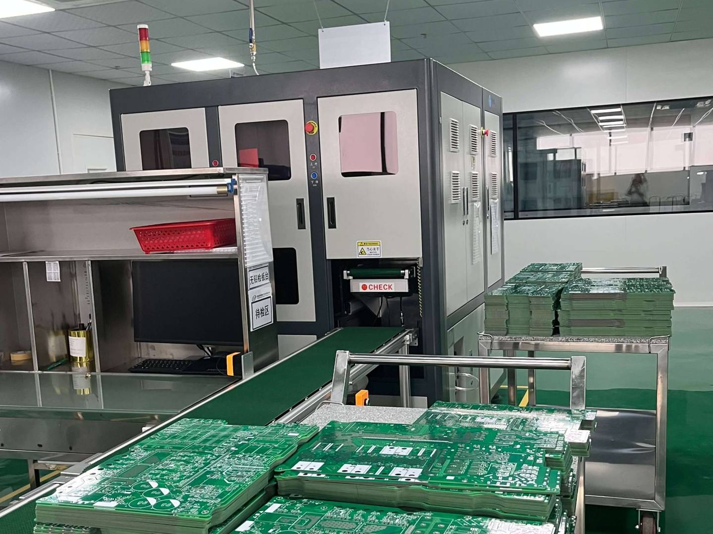
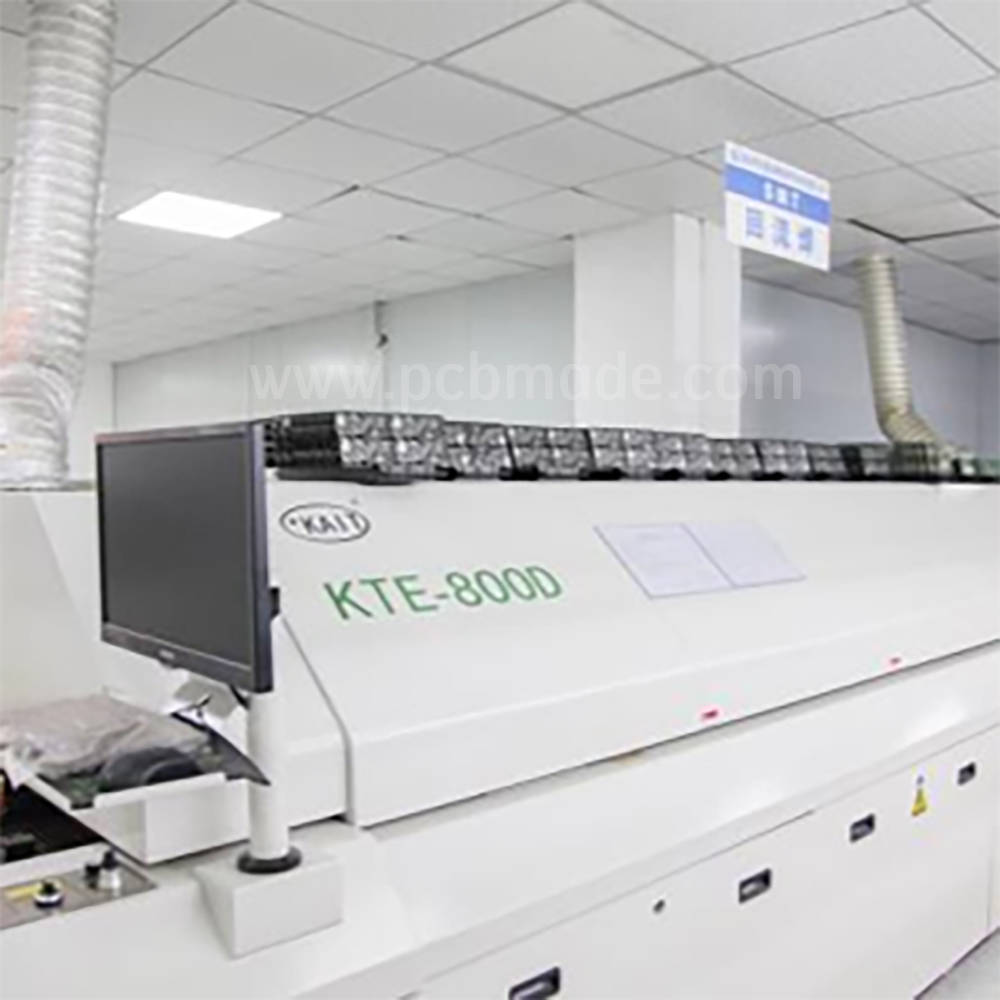

In the PCB manufacturing process, the molding process is the key link that determines the final shape and size of the PCB circuit board. Different molding methods have a direct impact on the production efficiency, cost control, and product quality of PCBs. Next, let’s take a look at the mainstream PCB molding methods and their applicable scenarios.
1. CNC molding:
CNC milling and forming is currently the most widely used PCB forming method. The principle is to cut the substrate along a preset path with a high-speed rotating milling cutter, which is suitable for processing irregular plates of any shape. The advantage of CNC lies in its accuracy of up to ± 0.1mm, which can handle complex contours and internal slotting, making it particularly suitable for small batch and multi variety production. However, limited by the single board processing mode, its efficiency is low and the tool wear cost is high. It is commonly used for high-density interconnect (HDI) boards, flexible circuit boards (FPC), and sample stage verification.
2 V-CUT board forming
V-CUT (V-shaped cutting) achieves rapid board separation by pre cutting V-shaped grooves between PCB panels and utilizing mechanical stress. This method has fast processing speed and can complete the segmentation of multiple spliced boards in a single operation, especially suitable for large-scale production of rectangular regular board shapes. Its cost is only one-third of that of CNC, but due to its linear cutting characteristics, it cannot handle curved edges. V-CUT needs to pay attention to residual burrs, and often requires secondary polishing after splitting. It is widely used in consumer electronics products.
3. Laser cutting forming
Laser cutting uses high-energy laser beams to vaporize materials, achieving contactless processing. Its accuracy can reach ± 0.05mm, with smooth and burr free incisions, making it particularly suitable for precision machining of brittle materials such as ultra-thin plates (below 0.2mm) and ceramic substrates. CO2 lasers are suitable for conventional substrates such as FR-4, while ultraviolet lasers can process polyimide flexible materials. Although the equipment cost is relatively high (about three times that of CNC), it is irreplaceable in high-end fields such as 5G millimeter wave antennas and medical micro devices.
4. Stamping forming
Stamping molding uses customized molds for high-speed cutting, and a single stamping can complete the formation of multiple PCBs, with a theoretical production capacity of up to 8000 times/hour. This process has extremely low marginal cost and is suitable for large-scale production of standardized products such as mobile phone motherboards and LED light boards. However, mold development costs are high (tens of thousands to hundreds of thousands of yuan), and modification is difficult, only applicable to orders with millions of pieces. The hydraulic die-cutting technology that has emerged in recent years has expanded the application boundaries of stamping processes by optimizing the mold structure to reduce the minimum aperture to 0.3mm.