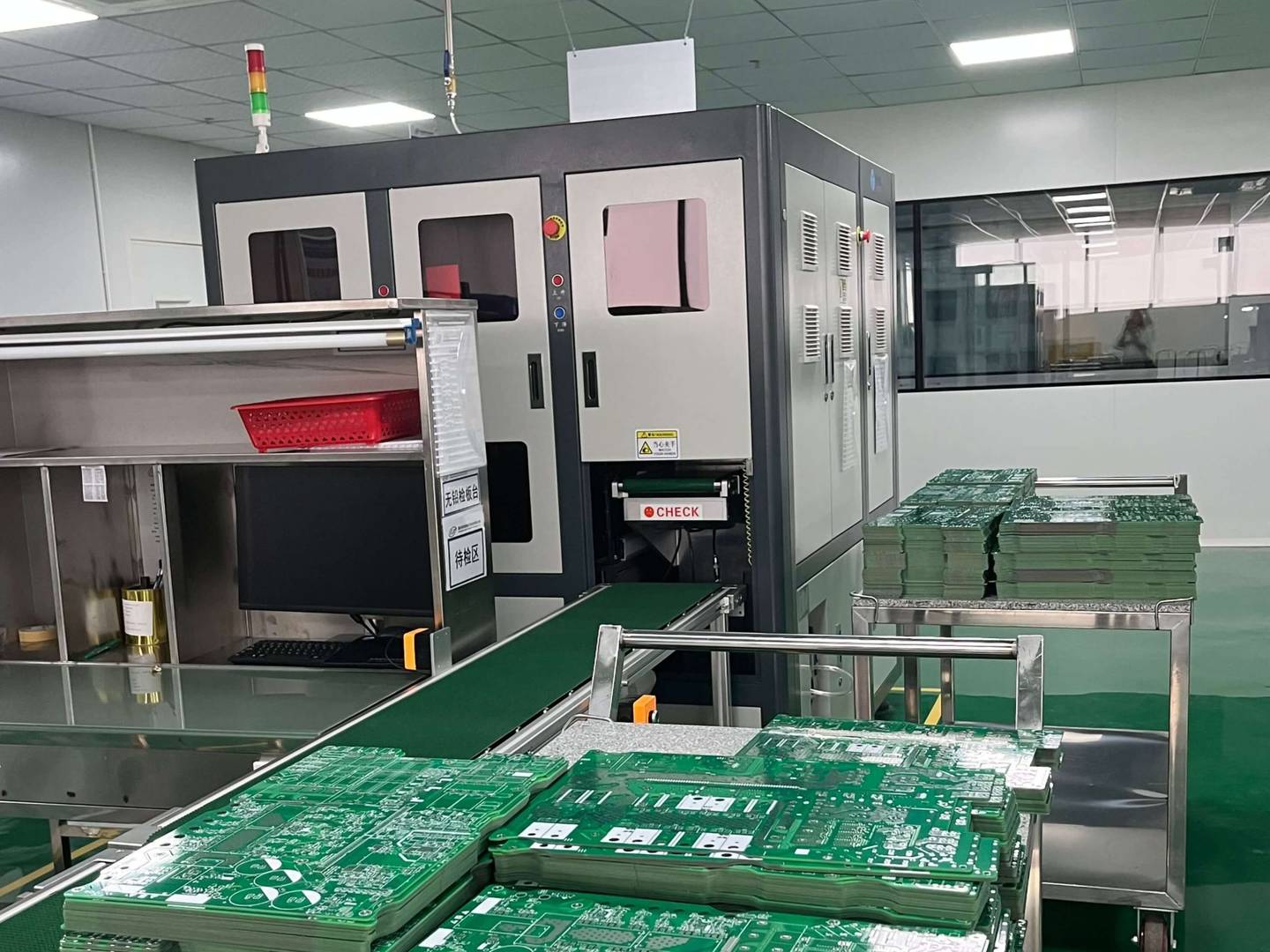

HDI circuit board is a high-density interconnect technology used to achieve more electronic components and connections in a limited space. This technology aims to improve the wiring density and performance of PCB (Printed Circuit Board) to meet the demands of modern electronic devices for smaller size, thinner and higher performance.
HDI (High Density Interconnect) circuit boards introduce more layers, smaller apertures, and tighter layouts in traditional circuit board designs. This enables HDI circuit boards to accommodate more components and connections in a relatively small size, thereby achieving higher functional integration and performance. It is usually achieved through the use of micro circuits, micro pores, and high-density interconnect technology.
HDI circuit boards are usually divided into the following types:
1. 1+N+1 HDI: This type of HDI circuit board has one standard board layer on each side and multiple non-conductive layers in the middle layer. This can increase the connection density and achieve more components in a smaller space.
2. 2+N+2 HDI: Similar to 1+N+1, but this type of HDI circuit board has a higher interconnect density. It includes two standard board layers and a non-conductive layer in the middle.
3. 3+N+3 HDI: This is a higher-level HDI design with more layers and higher connection density. It is suitable for very complex circuits and high-performance applications.
The design and manufacturing of HDI circuit boards require higher technology and precision. Due to the compactness of components and circuits, wiring is more challenging and requires the use of more advanced manufacturing technologies such as laser drilling, etching, and thin film deposition.
In short, HDI circuit boards are an advanced technology used to achieve higher density connections in limited spaces. It plays an important role in modern electronic devices, allowing more functions to be integrated into smaller sizes.