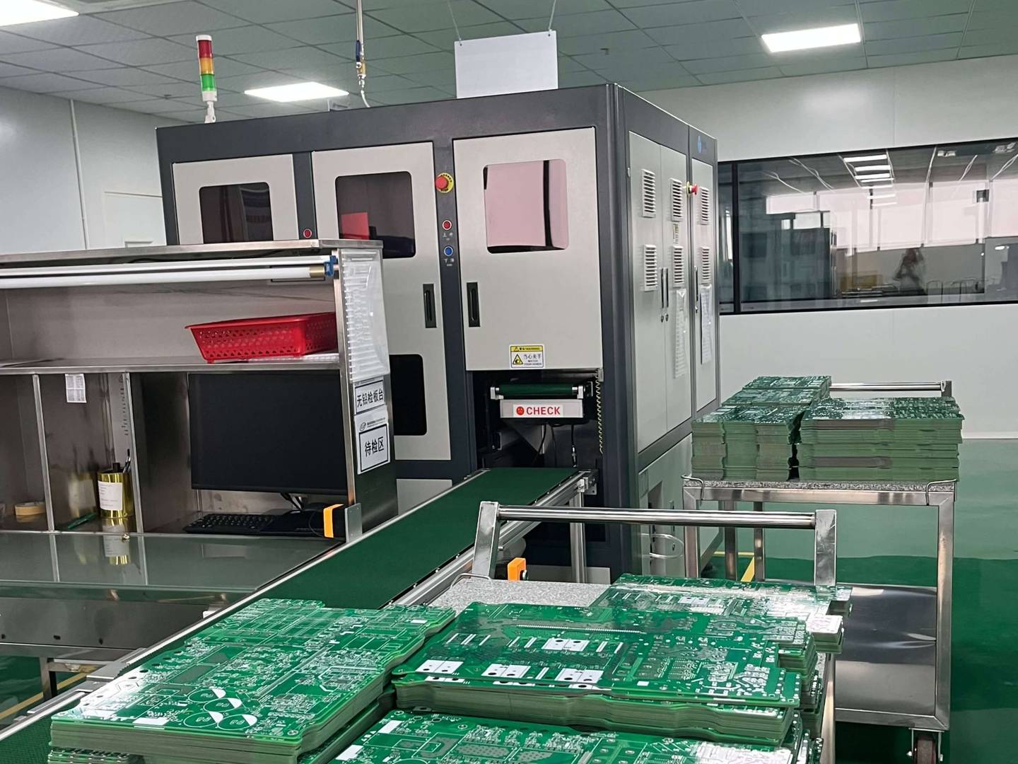

一、 What is a 6-layer PCB
A 6-layer PCB refers to a board with 6 different layers of circuits distributed on it. It consists of 4 internal layers and 2 external layers, with the internal layer made of copper foil located in the center of the board, and the external layer located at the top and bottom of the board. A 6-layer PCB is typically used for complex circuit designs because it can provide more space and reliability, while also improving the speed and quality of signal transmission.
二、 Introduction to the layering of 6-layer PCB
1. Top and bottom layers
The top and bottom layers are the two most common levels in a 6-layer PCB. They are typically used to place large components and connectors, and they are the surface of printed circuit boards. The main function of these two levels is to provide the structure and support of the circuit board, while also being used to connect external devices.
2. Internal Layer 1 and Internal Layer 2
Internal layer 1 and internal layer 2 are the two most important layers in a 6-layer PCB. They are typically used to place signal planes, power planes, and ground planes. The main function of these levels is to provide the electrical characteristics and signal transmission quality of the circuit board. They can reduce signal interference and noise, while also improving signal transmission speed and stability.
3. Internal Layer 3 and Internal Layer 4
Internal layer 3 and internal layer 4 are usually used to place signal and power lines. The main function of these levels is to connect different components and functional blocks, and provide more layout options. They can improve the reliability and performance of circuit boards, and reduce electromagnetic interference and noise.
三、 Stacking method of PCB
The stacking method of PCB refers to how different layers are combined together. There are two common stacking methods: symmetric stacking and asymmetric stacking. Symmetric stacking refers to placing inner layer 1 and inner layer 2 in the center position, and placing inner layer 3 and inner layer 4 on both sides respectively. This method can reduce the thickness and weight of the circuit board, while also improving the speed and quality of signal transmission. Asymmetric stacking refers to placing inner layer 1 and inner layer 4 in the center position, and placing inner layer 2 and inner layer 3 on both sides respectively. This approach can provide more layout options and electrical characteristics, while also reducing signal interference and noise.
四、 Methods for controlling impedance
Control impedance refers to the impedance value used to control signal transmission by designing the geometry and materials of a circuit board. This can improve the speed and quality of signal transmission, and reduce signal reflection and interference. Common methods for controlling impedance include: using parameters such as width, spacing, and thickness to control impedance values; Using differential circuits to reduce signal interference and noise; Use interlayer isolation to prevent signal crossover and interference.
A 6-layer PCB is a high-performance circuit board design that provides more space and reliability, while also improving the speed and quality of signal transmission. By introducing the design of 6-layer PCB, the stacking method of PCB, and the method of controlling impedance layer by layer, we can better understand the advantages and application scenarios of 6-layer PCB. In future electronic product design, 6-layer PCBs will play an increasingly important role.