In the microscopic world of electronic devices, PCB printed circuit boards play an important role in connecting various electronic components and constructing complex circuit systems. With the development of technology, PCB design is becoming increasingly precise, and the steel mesh layer, as a key link in the production process, plays an indispensable role in ensuring the manufacturing quality of circuit boards and improving assembly efficiency.
Basic structure of PCB circuit board
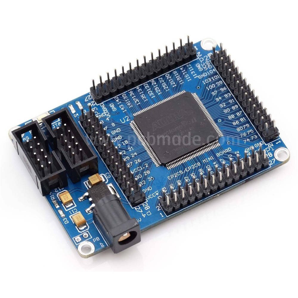
Before delving into the steel mesh layer, let’s briefly review the basic composition of PCB. PCB is mainly composed of insulating substrate, copper foil conductive layer, solder mask layer, silk screen layer, etc. Among them, the copper foil conductive layer is etched to form circuit patterns and serves as a carrier for electronic signal transmission; The solder mask is used to protect the circuit, prevent short circuits, and define the soldering area; The silk screen layer is used to label the position of components and circuit information.
Definition and production of steel mesh layer
Steel mesh, also known as SMT (Surface Mount Technology) template or solder paste printing template, although not directly part of the PCB structure, plays a crucial role in the PCB assembly process. Steel mesh is made of high-precision laser cut stainless steel sheets with holes or grooves corresponding to PCB pads, used for precise control of solder paste printing during SMT assembly.
The role of steel mesh layer
Accurate quantitative distribution of solder paste: In the first step of SMT assembly – solder paste printing, the steel mesh acts as a fine sieve to ensure that the solder paste can be evenly and accurately applied to the predetermined solder pad positions on the PCB, avoiding too much or too little, which is crucial for ensuring solder quality.
Improving welding quality: By precisely controlling the distribution of solder paste, steel mesh helps reduce welding defects such as bridging and void welding, improve welding consistency and reliability, and thus enhance the electrical performance of the entire PCB and the overall quality of the product.
Adapting to complex designs: With the trend of miniaturization and high density of electronic products, components on PCBs are becoming smaller and the spacing is becoming tighter. Steel mesh can be customized according to design requirements, and even small or irregular solder pads can be accurately matched to meet the needs of high-end electronic products.
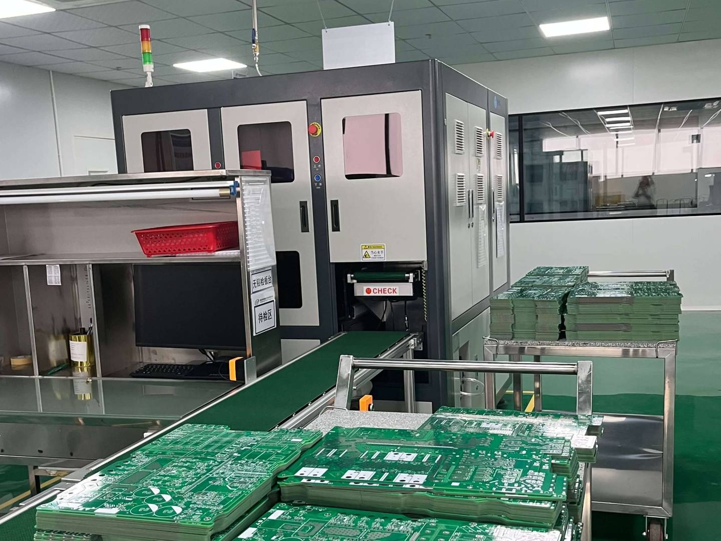
Improving production efficiency: In automated production lines, with the use of precision steel mesh and automatic solder paste printing machines, fast and efficient mass production can be achieved, greatly improving production efficiency and reducing the error rate of manual operations.
In summary, although the steel mesh layer does not directly form the physical structure of the PCB, it plays a crucial role in ensuring the accuracy, efficiency, and reliability of PCB assembly as a bridge between design and actual production in modern electronic manufacturing processes. With the continuous advancement of technology, the design and manufacturing of steel mesh will also become more refined and intelligent, continuously promoting the development of the electronic manufacturing industry. Understanding the role of the steel mesh layer is beneficial for us to gain a deeper understanding of the manufacturing process of electronic products and even promote technological innovation in related fields.


