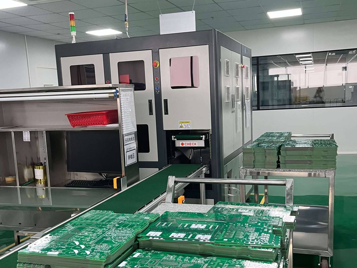

A six layer PCB board is a common electronic component connection board with a complex and diverse structure, suitable for various electronic products. Before delving into the structure of a six layer PCB board, we must first understand some basic knowledge. PCB board, also known as printed circuit board, is the basic substrate for electronic components, used to connect and support electronic components. A six layer PCB board consists of several layers of substrates made of different materials, interspersed with circuit layers and insulation layers.
Next, we will interpret the structure of the six layer PCB board layer by layer.
First layer: Top copper foil layer. The top copper foil layer is the surface layer of the PCB board, used to connect components and external signal pins. In general, the top copper foil layer will form circuit patterns through chemical corrosion or mechanical milling.
Second layer: Top layer circuit layer. The top layer circuit layer is one of the circuit pattern layers on the six layer PCB board, and is isolated by an insulation layer below it. In multi-layer PCB boards, the top circuit layer is usually used to connect circuits between components.
The third layer: inner circuit layer. In a six layer PCB board, there are usually multiple layers of inner circuit layers used to connect different circuits for signal transmission. The inner circuit layer is isolated by an insulation layer to avoid mutual influence between circuits.
The fourth layer: Ground Circuit Layer The ground circuit layer is used to connect the ground wires of various parts on the PCB board, playing a role in connection and conductivity. The design of the formation circuit layer is very important, as it can effectively reduce mutual interference between circuits during operation.
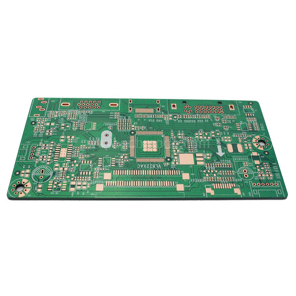
Layer 5: Bottom Circuit Layer The bottom circuit layer is usually used to connect circuits between different components on the PCB board, playing a role in signal transmission. The design of the underlying circuit layer needs to consider the layout and connection methods of components.
Layer 6: Bottom Copper Foil Layer The bottom copper foil layer is the bottom layer of the PCB board, used to connect components and external signal pins. The formation of the bottom copper foil layer also requires chemical corrosion or mechanical milling.
in summary,The structure of a six layer PCB board is complex, but each layer plays an indispensable role. Understanding the six layer PCB board structure is crucial for the design and manufacturing of electronic products.