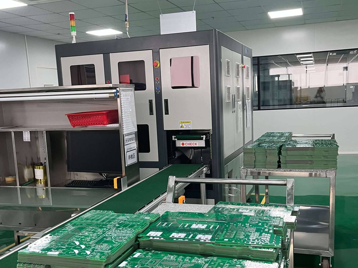

Firstly, let’s understand the definition of poor PCB appearance. Poor appearance of PCB refers to the phenomenon of defects, damage or non-compliance with requirements in the appearance during the PCB manufacturing process. These issues may lead to a decrease in the performance, reliability, or even malfunction of the circuit board.
So, what are the common problems with poor PCB appearance? Here are some situations we often encounter:
1. Pad cracking: Pad cracking may be caused by uneven temperature during the welding process, poor quality of welding materials, or excessive stress. This can lead to unstable soldering points, which may cause unstable or ineffective circuit connections.
2. Pinholes: Pinholes refer to tiny perforations on the surface of a PCB, usually caused by incomplete chemical reactions or material quality issues during the manufacturing process. Pinholes can cause uneven surface of circuit boards, reduce insulation performance, and even lead to short circuits.
3. Pad oxidation: Pad oxidation refers to the appearance of an oxide layer on the surface of a pad, usually caused by improper storage environment, poor material quality, or oxidation reactions during the manufacturing process. Pad oxidation can reduce the quality of welding, resulting in unreliable or even impossible connections at the welding point.
4. Copper foil peeling: Copper foil peeling refers to the separation of the copper foil layer on the surface of the PCB from the substrate, usually caused by poor adhesive, high temperature, or uneven pressure. Copper foil peeling can affect the conductivity of the circuit board, which may lead to abnormal signal transmission or circuit interruption.
The above are just some common problems with poor PCB appearance, and there are many other practical situations. So, what are the reasons for these problems? Let’s take a look at several main influencing factors:
1. Manufacturing process: Unreasonable or lax manufacturing processes can lead to poor PCB appearance. For example, improper control of temperature, pressure, and time, as well as incomplete chemical reaction processes, can all lead to appearance defects.
2. Material quality: Choosing low-quality substrate materials, welding materials, or adhesives will increase the risk of poor appearance. The quality of materials has a significant impact on the stability and reliability of PCBs.
3. Environmental factors: Temperature, humidity, and other factors in the manufacturing and storage environment can also affect the appearance of PCBs. Inappropriate environmental conditions may lead to abnormal chemical reactions, resulting in poor appearance.
In summary, poor PCB appearance is a common problem in the manufacturing process, which may have a negative impact on the performance and reliability of the circuit board. We need to pay attention to manufacturing processes, material quality, and environmental factors to ensure that the appearance quality of PCBs meets standard requirements.